Matmul Writeup
Yet another guy rediscovering the fundamentals of computer architecture through a simple math exercise.
Matrix multiplication is a simple algorithm: result[r][c] += left[r][k] * right[k][c]. So why is the simple implementation over 500x worse than the optimized one? The optimization is genuinely fascinating, touching over many core systems concepts, including caches, intrinsics, SIMD and multithreading.
What’s so special about matrix multiplication?
First off, it’s important to know about the nature of matrix multiplication and WHY they suffer so much a bad implementation despite the algorithm remaining the same complexity.
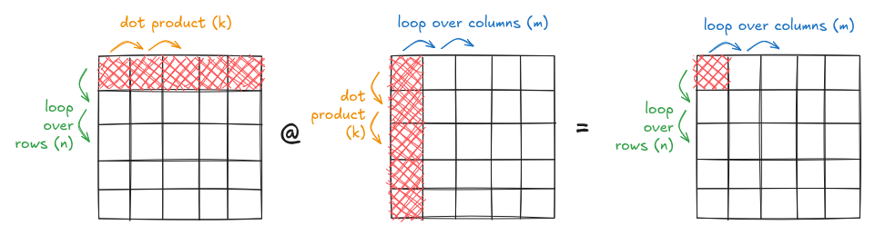
The operation takes in an n by k matrix, multiplies it with a k by m matrix to form a n by m.
In Big O Notation, the compute complexity can be expressed as \(O(n^3)\) while only needing \(O(n^2)\) memory. Each element is re-used n times, and it can be compute bound. However, that’s only possible if our implementation actually efficiently reuses the data. Our CPU’s compute speed outruns the DRAM feeding them data (known as memory wall). This means that we need to use our CPUs features through understanding vector registers, memory hierarchies, prefetching behaviors. And knowing these memory hierarchies and optimizing them genuinely does make a hundredfold difference.
Prelude: My System
I have an AMD Ryzen 9 9950X, on the Zen 5 architecture, featuring 16 cores and (most importantly) the latest AVX512 SIMD instructions. It has a base clock of roughly 4.3 GHz, and seems to sustain roughly ~4.9 GHz when OpenBLAS is doing matrix multiplication.1
1 Desktop chips genuinely can run fast, and my system uses features like PBO to unlock power consumption and undervolts if you’re curious how I can sustain these clocks. Datacenter chips that are probably better suited to run these kinds of computation workloads will have an insane amount of cores at the expense of clock speeds 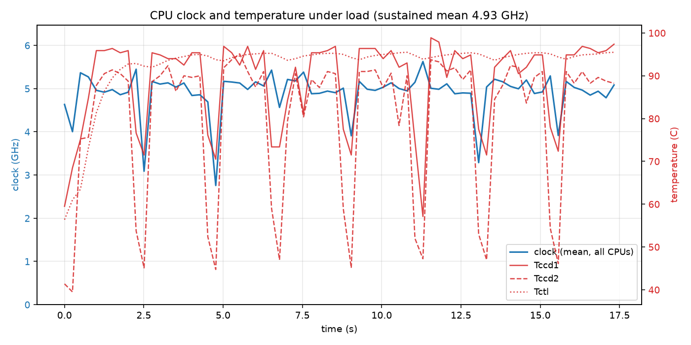
Matrix multiplication heavily uses SIMD (Single Instruction, Multiple Data) which allows us to do many floating point operations at once. For 32-bit floats on AVX512, thats 512 / 32 = 16 floats at once.
| Instruction | Latency | Throughput | Uops | Ports |
|---|---|---|---|---|
| VFMADD231PS (ZMM, ZMM, ZMM) | 3/4 | 0.50 | 1 | 1*FP0/1 |
2 Documentation has a latency of 4, but measured is 3. I’ll assume 4 for worst-case.
Specifically, we can use the VFMADD (vector fused multiply-add) which does \(a * b + c\), allowing us to do 2 operations for one instruction. With a throughput of 0.5 cycles / instructions, we can issue 2 of these in parallel every cycle.
So, theoretically, the total FLOPS is
\[ \underbrace{4.9\times10^{9}}_{\substack{\text{cycles/s} \\ \text{\scriptsize measured}}} \;\times\; \underbrace{2}_{\substack{\text{FMA/cycle} \\ \text{\scriptsize 2 FP pipes}}} \;\times\; \underbrace{16}_{\substack{\text{lanes/FMA} \\ \text{\scriptsize 512b ÷ 32b}}} \;\times\; \underbrace{2}_{\substack{\text{flops/lane} \\ \text{\scriptsize mul + add}}} \approx 314\, \text{GFLOP/s} \]
per core! With 16 cores, its roughly \(\approx 5\, \text{TFLOP/s}\). Crazy considering GPUs, dedicated units for matrix multiplications, like my 3060 can do 12.74 TFLOPS of FP32, which is not the 100x speedup that I would’ve assumed.3
3 This is an extremely an unfair comparison for the GPU, which can hit 3x that on dedicated “tensor cores” as well as having 4x more memory bandwidth. Also, the 3060 is an incredibly old and low-end GPU (compared to the rest of the RTX-series lineup). Still, incredible to see how much computation these general purpose machines can do!
Me vs. OpenBLAS
Benchmarked using Google Benchmark. Tested using GoogleTest, against OpenBLAS’s output. Float comparisons are done with a relative tolerance of 1e-2 and an absolute tolerance of 1e-3, consistent with OpenBLAS’ testing methods
#todo
| Implementation | Time (ms) | GFLOPS | % of OpenBLAS |
|---|---|---|---|
| OpenBLAS for 1024x1024 (single-threaded) | 6.61 | 325 | |
| Naive (1024 x 1024) | 269 | 7.98 | |
| Cache Aware (1024 x 1024) | 26.0 | ||
| OpenBLAS (4096x4096, single-threaded) | 414 | 332 | |
| OpenBLAS (4096x4096) | 43.7 | 3142 | |
| OpenBLAS (4096x4096, tuned with 16 threads + taskset) | 34.4 | 4001 | |
| Register Tiling (4096x4096) | 964 | 143 | 43.07% |
| Full Tiling (4096x4096) | 636 | 216 | 65.06% |
| Full Tiling + Packing (4096x4096) | 503 | 273 | 82.23% |
| Full Tiling + Optimized sequential packing (4096x4096) | 437 | 315 | 94.88% |
| Full Tiling + Optimized sequential packing + Threading (4096x4096) | 33.4 | 4120 | 103% |
Note: single threaded is higher than calculation due to AMD chip’s behavior of being able to boost up to ~5.4 GHz for a single core due to less thermal constraints
Basic Implementation
The naive approach. This one implements matrix multiplication as its literal definition: for each row of A and column of B, compute their dot product. 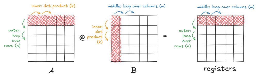
void naive(int M, int N, int K, const float *A, const float *B, float *C) {
  for (int r = 0; r < M; r++) {
    for (int c = 0; c < N; c++) {
      float acc = 0.0f;
      for (int i = 0; i < K; i++) {
        acc += A[r * K + i] * B[i * N + c];
      }
      C[r * N + c] = acc;
    }
  }
}
4 Why do we use a float for an accumulator and only update the matrix at the end? This allows us to use a register to store our results, and only write to memory once its done. Foreshadowing for later… :)
We’re compiling with -O3 -march=znver5 to enable AVX512 (gcc is conservative, and doesn’t assume AVX512 since not all computers have those) and let the compiler speed up some of our hot loops to not pay a branch predictor cost.
Brief Dive into Cache
There’s a simple fix that can 10x our performance.
CPUs have a region of specialized memory that’s meant to be faster, known as cache. It lives on the die itself, sitting right next to the compute cores for maximum speed & bandwidth. This was directly to give CPUs the fast-speed memory it needs to consume for its operations, but they are much smaller than RAM.
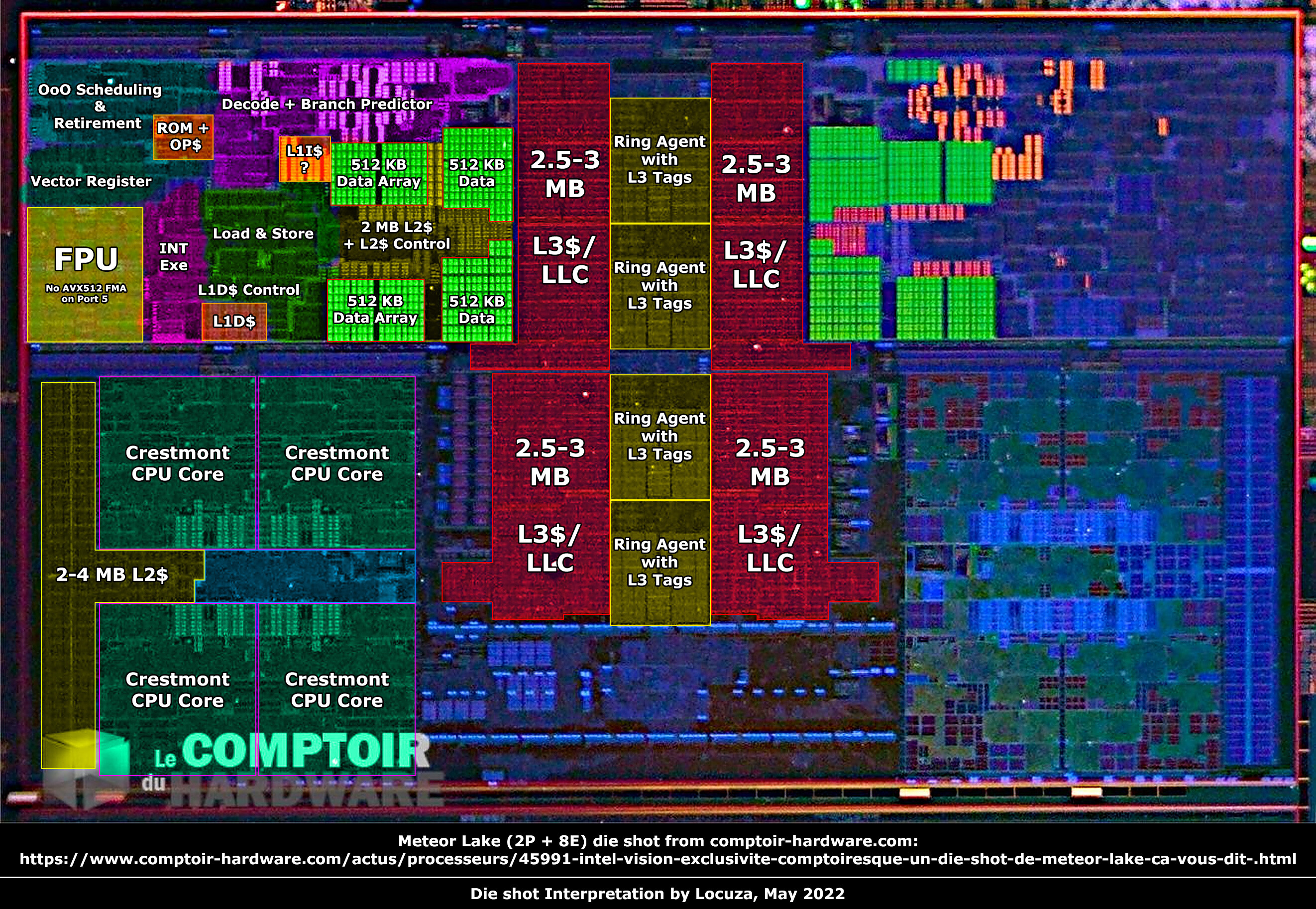 Credit: https://twitter.com/Locuza_/status/1524441315441786881/. Die shot is of a different chip, but it illustrates my point
When you fetch a single element from memory, the CPU automatically fetches the whole cache line of 64 bytes and puts it into cache. In addition, instead of waiting for memory to arrive, CPUs automatically run prefetchers to try and predict what memory you’ll use next. This makes sequential access very cache-friendly and more performant, because you utilize the entire 64 bytes that the CPU automatically fetches for you and the prefetcher guesses the memory you need next correctly.
And the implementation is as simple as switching around a loop. And now, in our hot loop, we’re going across the matrix, which is a sequential walk down memory.
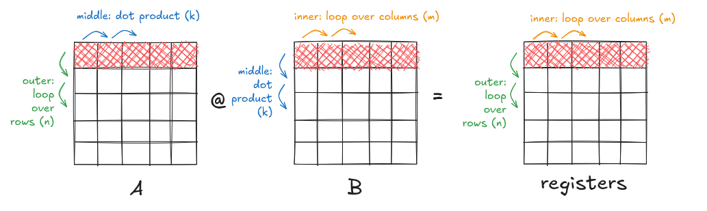
Which is just rearranging one line of code:
void cache_aware(int M, int N, int K, const float *A, const float *B,
                 float *C) {
  for (int r = 0; r < M; r++) {
    for (int i = 0; i < K; i++) {
      for (int c = 0; c < N; c++) {
        C[r * N + c] += A[r * K + i] * B[i * N + c];
      }
    }
  }
}
And looking at the assembly in godbolt.org:
vmovups zmm0, ZMMWORD PTR [rcx+rax]
vfmadd213ps     zmm0, zmm1, ZMMWORD PTR [rdx+rax]
vmovups ZMMWORD PTR [rdx+rax], zmm0
the compiler was smart enough to vectorize it automatically! Another, indirect benefit of sequential memory access5.
5 Sequential access patterns will come up as a theme a lot for optimization.
And with that simple swap of one line of code, we’re at 10x of our naive examples!
Not all Memory is Equal
While technically not a cache, the fastest memory of them all are registers, which CPUs use internally for their operations. We can use this to our advantage. Zen5 has 32 zmm registers, each holding 512 bits, totaling 2KB of info we can store!
Our previous example required loading and storing constantly to (cached) memory. However, we can further improve it by storing as much as we can into the 2KB of memory.
Since matrix multiplication is (m x k) by (k x n) = (m x n) operation. Since the same (3x99999) matrix and (99999x3) matrix end up getting reduced to (3x3), a good idea would be to use registers as our result tile, and accumulate A @ B into that register tile. This gives us the most reuse, since we can loop across K, and we want to spend our precious registers on something that can be reused often.
So how do we use zmm registers to speed up the actually A @ B process? If we express matrix multiplication in a math way,
\[ \begin{bmatrix} a & b & c \\ d & e & f \\ g & h & i \end{bmatrix} \begin{bmatrix} j & k & l \\ m & n & o \\ p & q & r \end{bmatrix} = \begin{bmatrix} aj+bm+cp & ak+bn+cq & al+bo+cr \\[4pt] dj+em+fp & dk+en+fq & dl+eo+fr \\[4pt] gj+hm+ip & gk+hn+iq & gl+ho+ir \end{bmatrix} \]
We can see that the first row is the sum of \(a \cdot \begin{bmatrix} j, k, l \end{bmatrix} + b \cdot \begin{bmatrix} m, n, o \end{bmatrix} + c \cdot \begin{bmatrix} p, q, r \end{bmatrix}\) The second row is \(d \cdot \begin{bmatrix} j, k, l \end{bmatrix} + e \cdot \begin{bmatrix} m, n, o \end{bmatrix} + f \cdot \begin{bmatrix} p, q, r \end{bmatrix}\) The third row is \(g \cdot \begin{bmatrix} j, k, l \end{bmatrix} + h \cdot \begin{bmatrix} m, n, o \end{bmatrix} + i \cdot \begin{bmatrix} p, q, r \end{bmatrix}\)
So if we were to extend this example to 1024-sized matrixes, we could: 1) loop through each element of A 2) broadcast (copy-paste) it into a vector of 16 elements 3) load the corresponding row of B into zmm registers 4) perform a fast FMA into the register accumulator
This is still slow however. Zen5 has 2 load ports, meaning it can perform 2 512-bit loads per cycle. Each broadcast is a load, and 16 floats from B is another load. That lets us do 1 FMA/cycle, which is half of our peak limit at 2 FMAs/cycle.
But there’s one more trick we can use. See how rows of B are reused for different elements? Instead, what we can do is load a single row of B within zmm registers, and then FMA them into our register accumulator. Then we go down a row in A, and repeat against the same row. 6 Once again, optimizing registers for data that can be re-used.
6 This contradicts the sequential memory rule I was talking about earlier, but theres an optimization we’ll do later down the line to turn it back to sequential. Right now, being able to do more than 1 FMA/cycle will be much faster than any cache level speed up we can get.
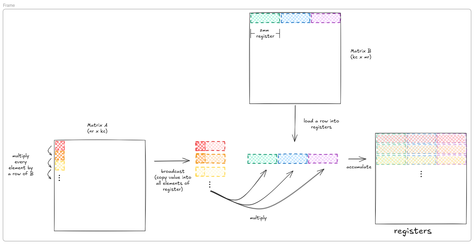
In code, it looks like this. It heavily uses compiler intrinsics to achieve this register-level behavior we’ve been describing. It uses templates so the compiler can unroll them into a continuous stream of instructions. Pretty cool what the compiler can do when you get specific enough! Saves us from writing the assembly.
// Its technically row by (columns * 16).
template <int m_reg, int n_reg_zmm>
inline void register_accumulator(int k_cache, const float *left, const int lda,
                                 const float *right, const int ldb,
                                 float *result, const int ldc) {
  __m512 acc[m_reg][n_reg_zmm];

  /*
  // Fill registers with zero
  for (int r = 0; r < rows; r++) {
    for (int c = 0; c < columns; c++) {
      acc[r][c] = _mm512_set1_ps(0.0f);
    }
  }
  */

  // Fill registers with the result
  for (int r = 0; r < m_reg; r++) {
    for (int c = 0; c < n_reg_zmm; c++) {
      acc[r][c] = _mm512_load_ps(result + r * ldc + c * 16);
    }
  }

  for (int i = 0; i < k_cache; i++) {

    // Load `columns` registers of `right`
    __m512 right_row[n_reg_zmm];
    for (int c = 0; c < n_reg_zmm; c++) {
      right_row[c] = _mm512_load_ps(right + i * ldb + c * 16);
    }

    // Actual matmul
    for (int r = 0; r < m_reg; r++) {
      __m512 el = _mm512_set1_ps(left[r * lda + i]);

      for (int c = 0; c < n_reg_zmm; c++) {
        acc[r][c] = _mm512_fmadd_ps(el, right_row[c], acc[r][c]);
      }
    }
  }

  // Move registers into memory
  for (int r = 0; r < m_reg; r++) {
    for (int c = 0; c < n_reg_zmm; c++) {
      _mm512_store_ps(result + r * ldc + c * 16, acc[r][c]);
    }
  }
}
This is known as the microkernel.
Since we have limited registers, we will subdivide the matrix into smaller dimensions \(n_{reg}\), \(m_{reg}\) and \(k_{cache}\) that the microkernel can use.7
7 We’ll explain why this is called k_cache and not k_reg later. But notice that register count doesn’t depend on k_cache at all, since we loop across it
By using more registers, we can break through the 2 loads/cycle limit and start doing more FMAs per load. Each iteration of our inner loop needs to load \(n_{reg} / 16\) zmm registers, after which we do \(m_{reg}\) loads and \(m_{reg} \times n_{reg}\) FMAs. So our loads/FMA is really \(\frac{n_{reg} + m_{reg}}{m_{reg} \times n_{reg}}\), and as long as that number is \(<1\), we’re not being limited.
In addition, since it takes 4 cycles of latency (meaning we need to wait 4 cycles before performing another FMA to accumulate on a single register of a register tile), we need \(m_{reg} \times n_{reg}\) to be greater than 8 (4 cycles of latency @ 2 FMA/cycle). Pretty much any sensible value we pick will hit this threshold, but it’s something I thought would be interesting to mention.
Since we have only 32 registers, we need to be careful of our \(m_{reg}\) and \(n_{reg}\) values. The register tile uses \(m_{reg} \times n_{reg}\) registers, and we need to load in a full \(n_{reg}\) zmm registers for a column, and at least one register for the broadcasting. So in total, we need \((m_{reg}+1) \times n_{reg} + 1\) registers.
We’re going to use 8 x 32 tiles because it divides easily into 1024, and I don’t want spill-over handling complicating the code (not as interesting IMO)8
8 I also considered 4x64, but the performance was worse. Of course, the best implementations would use something like 12x32. I assumed it wouldn’t have made a huge difference since we’re approaching the FMA/cycle limit, and the spill-over might actually make my code slower. But that’s just analytical thinking. In the future if I ever revisit this, I will test this out.
So now all that remains is to subdivide our 1024 matrix into strips of 8 and columns of 32, and loop across those.
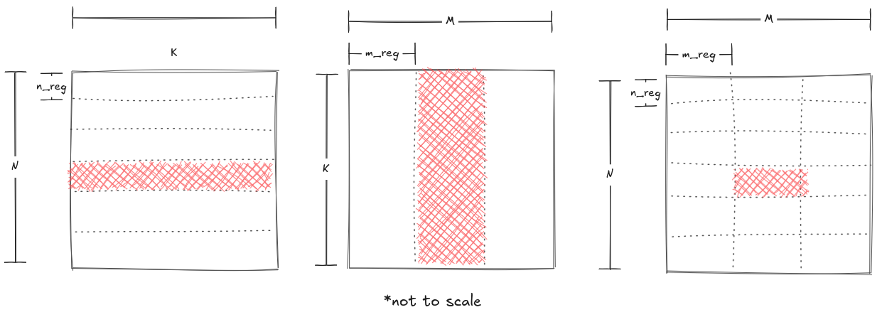
Here’s what the code looks like:
void register_tiling(int M, int N, int K, const float *A, const float *B,
                     float *C) {
  constexpr int splitRows = 8;
  constexpr int splitCols = 32;

  for (int c = 0; c < N; c += splitCols) {
    for (int r = 0; r < M; r += splitRows) {

      register_accumulator<splitRows, splitCols / 16>(K, A + r * K, K, B + c, N,
                                                      C + r * N + c, N);
    }
  }
}
Tiling & Blocking:
The small \(m_{reg}, n_{reg}\) accumulator we have created is called the microkernel. Those 2 loops around the microkernel is called the macrokernel.
The microkernel is highly optimized, but once again, it depends on our memory bandwidth to keep supplying it with enough data to saturate those FMAs.
for (int i = 0; i < inners; i++) {
    // Load `columns` registers of `right`
    __m512 right_row[columns];
    for (int c = 0; c < columns; c++) {
      right_row[c] = _mm512_load_ps(right + i * ldb + c * 16);
    }

    // Actual matmul
    for (int r = 0; r < rows; r++) {
      __m512 el = _mm512_set1_ps(left[r * lda + i]);

      for (int c = 0; c < columns; c++) {
        acc[r][c] = _mm512_fmadd_ps(el, right_row[c], acc[r][c]);
      }
    }
}
So per k-step, we load \(n_{reg} * 16 + m_{reg}\) floats. Each step, we perform \(n_{reg} \times m_{reg}\) FMAs.
At \(n_{reg}\) = 64, \(m_{reg}\) = 4, we load 256 bytes / 8 cycles = 32 bytes / cycle = 156.8 GB/s. This far exceeds DRAM at a theoretical peak of 90 GB/s910
9 That’s also not accounting for the fact it’ll need 160 GB/s per CORE, whereas this DRAM number is for the entire CPU.
10 6000 MT/s
11 Or also referred to as blocks.
This means that we need to optimize our macrokernel’s data to fit into cache. However, we still have to consider cache sizes. When the matrices get bigger, we need to start working on small sub-matrices that we load into cache at a time. We’ll call these sub-matrices “tiles”11. This technique of working on smaller sets is called tiling or blocking.
And since our implementations are getting faster, we can bump up to 4096 x 4096 matrices. This also would expose any flaws in our tiling, as our previous 1024 x 1024 matrices needed 4MB of RAM each (12MB total), which would easily fit in L3 cache. 4096 x 4096 matrices consume 64 MB each, and 192MB would easily blow through all caches.
The first unbounded dimension we have is k, which we use in the microtile. Now that we have a bigger matrix, look at how our cache behaviors change:
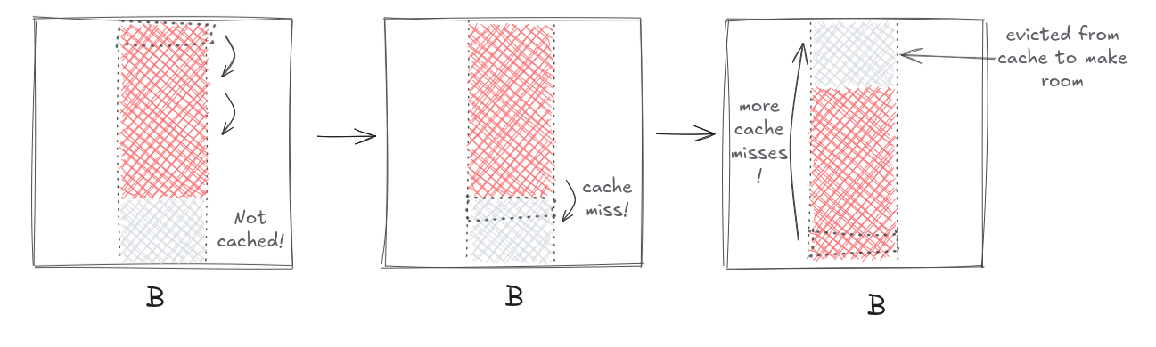
Our register tiling splits B into tiles of 64 by \(K\), where \(K\) is the inner dimension of the matrix, meaning it can be arbitrarily large. The issue that occurs is that our cache doesn’t have enough space to put all of the tile of B. Since caches work on an LRU-ish (least recently used policy), it will start evicting the elements we haven’t visited in a while - which are actually the elements we are about to visit! This causes a lot of misses, which will require fetching from slower memory. Since this is the hottest (innermost) loop, a cache miss here would be significant.
Instead, we can introduce a tiling factor. We’ll call this \(k_{cache}\), and we’ll split the blocks into size of \(k_{cache}\)
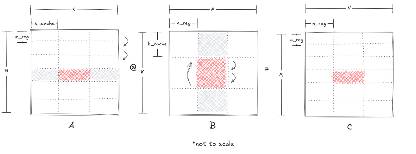
And now, we only load a smaller segment of the entire column and we can reuse that, as we stride down the rows of A.
Note that this comes at the cost of no longer having all of C in a register, instead, C will have to be update \(K \div k_{cache}\)
However, let’s zoom out to our macrokernel. Similarly, our \(M\) and \(N\) are not bounded. And since we upgraded our size to 4096 x 4096, we face this problem: 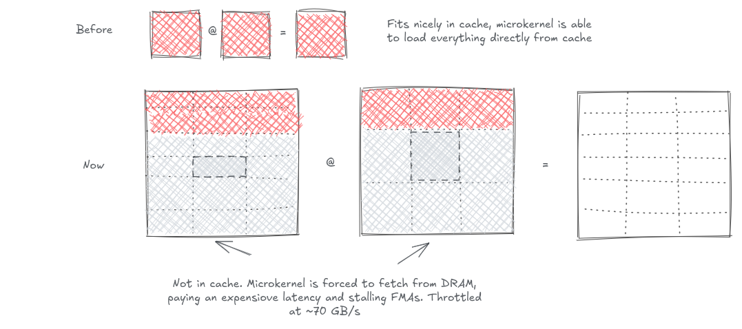
So we can apply that K-tiling approach on both \(M\) and \(N\), to achieve full 2D-tiling 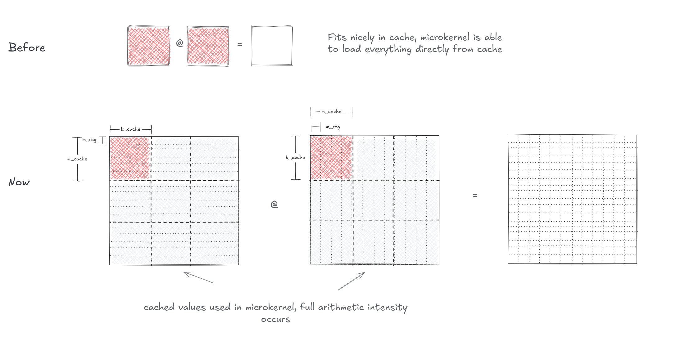
This way, everything is in cache. We now have to determine what order to loop through the tiles in (remember, order matters!) and pick the right values for \(m_{cache}, n_{cache}, k_{cache}\). But how?
Not all Cache is Equal
First, we have to understand that cache isn’t one-size-fits-all. The faster the cache, the less dense it is, and the more precious die space it wastes. So CPUs split them up into 3 tiers, L1d12, L2, L3, each having worse bandwidth & latency than the previous, but more capacity. L1 and L2 are per-core, while L3 is shared between each CCD13
12 L1 cache is split up into the instruction and the data cache. Yes, memory is so slow even the CPU instructions in memory have to be cached or it would stall at 5GHz
13 The 9950x is made up of 2 separate dies, called Core Complex Die, stitched together. It seems that they cannot share the L3 cache between CCDs (source)
| Cache Level | Amount |
|---|---|
| Registers | 32 zmm (512-bit) registers, totaling 2048B |
| L1d | 48K |
| L2 | 1M |
| L3 | 32M |
Keep in mind cache behavior: anytime you access memory, it first looks at L1. If that misses it goes to L2, then L3, and then finally DRAM. Anything that gets pulled will always end up in L1 cache, which is important to consider for later.
Cache Derivation from Scratch
Look at our macrokernel loop:
for (int c = 0; c < N; c += splitCols) {
    for (int r = 0; r < M; r += splitRows) {

      register_accumulator<splitRows, splitCols / 16>(K, A + r * K, K, B + c, N,
                                                      C + r * N + c, N);
    }
}
If we look at our macrokernel’s inner loop. We pick a column, and then loop through ALL the rows, performing the microkernel. What’s happening is we are reusing one strip, while streaming (using, discarding, moving onto the next) across the entire other matrix.
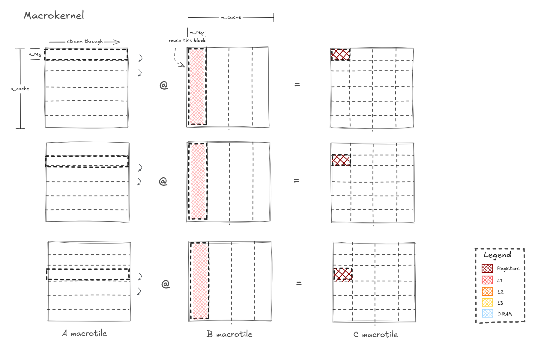
Consider two possible implementations. We can swap which one belongs on the outer loop. But which is better?
loop n / n_reg times:
    // B microtile in L1 cache, reuse across inner loop
    loop m / m_reg times:
        // Stream through the A microtile
        read m_reg * k floats
loop m / m_reg times:
// A microtile in L1 cache, reuse across inner loops
loop n / n_reg times:
// Stream through the B microtile
read n_reg * k floatsSince we’re reusing the data, its best we keep it in the fastest possible cache, the L1, because it will make subsequent reads fast. However, we stream the other piece, meaning that it should go in a slower level.
They both loop the same amount of times (order doesn’t change that), but we read different amounts of floats depending on how we loop. And memory bandwidth is a problem for us, we want to choose the loop that minimizes the amount of streams. Since our \(m_{reg} \ll n_{reg}\), we should choose columns as the outer loop, and rows as the inner loop. Another way of thinking about this is that we are forced to re-read either A or B. Since n = 32 and m = 8, we have to do less full re-reads when striding by 32’s. In general, since \(n_{reg}\) has to be a multiple of 16, due to AVX512, it will very likely end up bigger.
So which tier of memory should A go into?
Let’s continue work our way bottom up. Look at the very outer loop: when we get to the next micro-column, we repeat the loop across all rows. We see that the A macrotile is being reused, so it should actually go in the L2 cache.
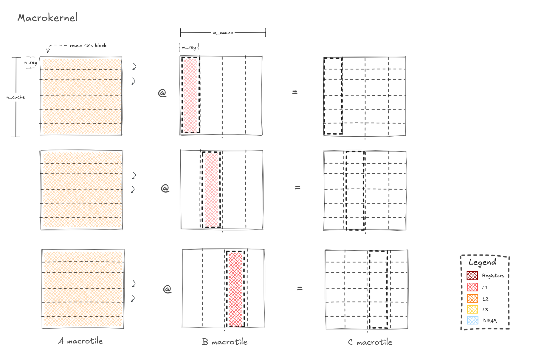
So that’s how we derived the two loops here:
for (int c = 0; c < N; c += splitCols) {
    for (int r = 0; r < M; r += splitRows) {

      register_accumulator<splitRows, splitCols / 16>(K, A + r * K, K, B + c, N,
                                                      C + r * N + c, N);
    }
}
Loop over r to keep the B microtile reused, and then loop over c to keep the A macrotile reused.
Now stepping out into the full kernel. Since our internal loop has already read the entire B panel, it would make sense to continue reusing it. So we put the B macrotile in L3 cache. 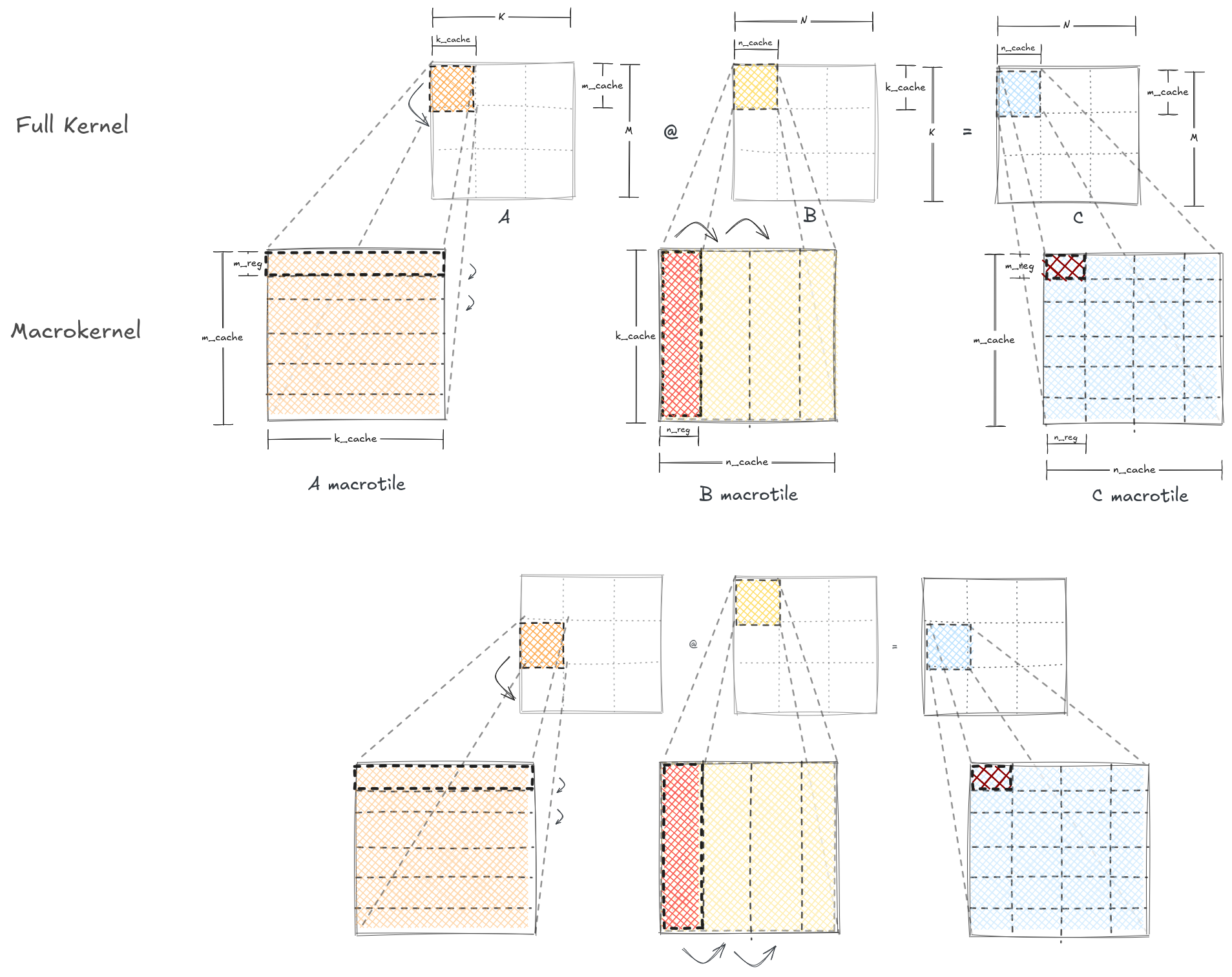
So that means the next level should once again, loop across rows.
for (int rc = 0; rc < M; rc += splitRowCache) {
    // Macrokernel
    for (int c = cc; c < cc + splitColCache; c += splitColRegisters) {
        for (int r = rc; r < rc + splitRowCache; r += splitRowRegisters) {

        // Microkernel
        register_accumulator<splitRowRegisters, splitColRegisters / 16>(
            splitInnerCache, left + r * K + kc, K, right + kc * N + c, N,
            result + r * N + c, N);
        }
    }
}
Here’s another view of how the caching works, courtesy of “Analytical Modeling Is Enough for High-Performance BLIS” 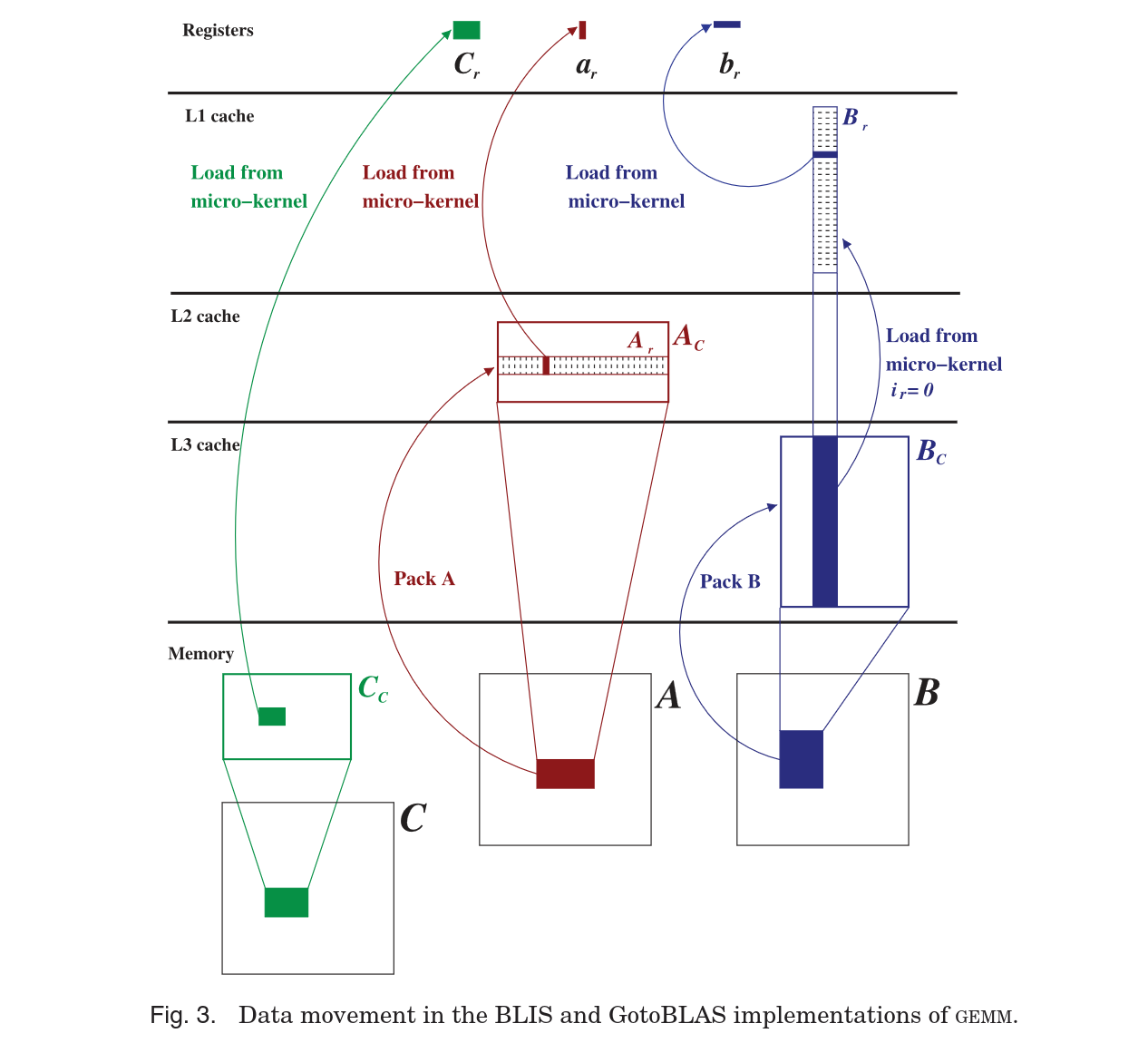
The last two loops have to loop over k_cache or n_cache. n-cache being the outer loop is the right choice here, since it allows the C tile to be re-used across k_cache iterations. Also allows for better parallelism (which we’ll see later!)14
14 Spoiler: it’s because paralleizing K will cause threads to access the same sections of C, which will be really bad for perfomance if we need to introduce atomics & locking.
Optimizing the parameters
Let’s summarize the values we have.
| Memory Tier | What’s in it | Size |
|---|---|---|
| Registers | The accumulator tile of size m_reg x n_reg, row of B in registers | 32 zmm registers |
| L1d | B micropanel of size k_cache x n_reg A micropanel will be streamed here, account for it C will also be passed through here as it’s written |
48KB |
| L2 | A panel: m_cache x k_cache | 1MB |
| L3 | B panel: \(k_{cache}\) x \(n_{cache}\) | 32M |
| DRAM | Full A, B | Irrelevant |
For L1d, it’d make sense we want to pick a k_cache that maximizes the space. But we have to account for A microtile being streamed. C will also be in L1 as its written to. So we need to keep 1 way for both. The total size we should allocate is then (12 ways - 2) x 64 lines x 64B = 40960B
So k_cache can be as high as 40960 / 32 / 4 = 320. We’ll pick 256 as it divides cleanly.
So m_cache can be 1024. But parallelism beats all so we’d much rather have < 512 to saturate the cores.
So n_cache can be well 4096. We’ll go with these numbers, and then implement an auto-tuner at the end when we have the remaining optimizations in place
Just pack it up…
A brief dive into how cache’s really work.
Throughout the entire optimization, we have been ignoring a critical property of caches: that they’re not fully associative.
Caches need some way to know which line refers to which memory address so that they can retrieve it later. On one end, you have direct-mapped, where a memory addresses must belong in a “slot”15 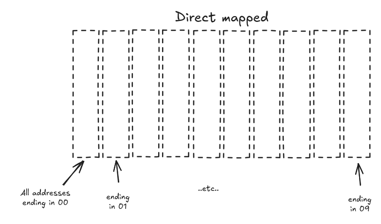
15 Implemented using modular arithmetic
16 for instance, in specific 2D array sizes where each column would map to the same “block”
This approach is very simple to look up (just a modulo), but has a severe problem: conflicting addresses overwrite each other. If you’re dealing with only addresses that map to the same slot16 you end up not using much of your cache.
On the other end, you have fully associative, which means any address can go anywhere. 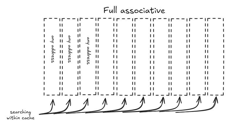
But now searching requires looking through every cache line, which is O(n). So in order to hide the latency, hardware would need to do all O(n) comparisons in parallel, which would a) be huge power consumption and b) probably impossible with that many lines.
So modern hardware settled on the middle-ground, set associativity. The cache is sectioned off within directly mapped blocks, called sets, but within each set, it is fully associative. The number of distinct addresses a set can store is called the number of ways. It can also be called N-way associative cache, where N is the number of ways
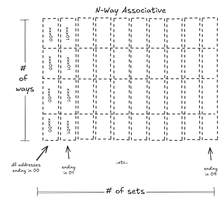
So now a search can narrow down to a set, and then run the O(ways) comparison in parallel. This allows for some amount of conflicts.
For my machine
> lscpu -C
NAME ONE-SIZE ALL-SIZE WAYS TYPE        LEVEL  SETS PHY-LINE COHERENCY-SIZE
L1d       48K     768K   12 Data            1    64        1             64
L1i       32K     512K    8 Instruction     1    64        1             64
L2         1M      16M   16 Unified         2  1024        1             64
L3        32M      64M   16 Unified         3 32768        1             64
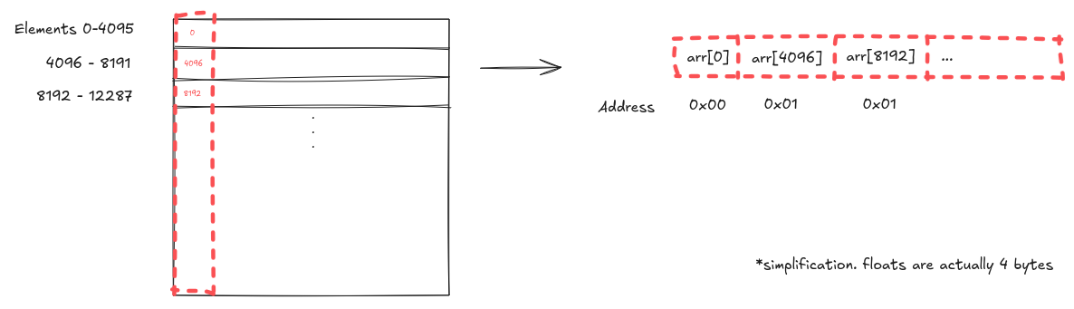
And here’s the problem: with 64 sets at a line of 64B, that means every address 4096 bytes apart belong in the same set. So every time we go down a column in our 4096x4096 matrix, we’re actually striding down 4 x 4096 bytes. So despite being completely different addresses, they’d end up in the same set and constantly evict each other, leaving the rest of the 63 sets untouched.
The solution? To copy the data into a scratch buffer, which would hide the ugly multiple-of-4096-byte stride. Sounds counterintuitive and seems to be a waste of time, but genuinely is worth it given how much faster the cache is. Matrix multiplication is also a special problem, since it’s n^3 ops on n^2 data, it is worth this copying.17
17 After all, copying is a read + write. So as long as we read from the packed data > 2 times, it’s worth the cost
void full_tiling_packing(int M, int N, int K, const float *A, const float *B,
                         float *C) {
  constexpr int splitRowRegisters = 8;
  constexpr int splitColRegisters = 32;

  constexpr int splitRowCache = 256;
  constexpr int splitColCache = 4096;
  constexpr int splitInnerCache = 1024;

  float *packA = (float *)aligned_alloc(64, splitRowCache * splitInnerCache *
                                                sizeof(float));
  float *packB = (float *)aligned_alloc(64, splitInnerCache * splitColCache *
                                                sizeof(float));

  for (int cc = 0; cc < N; cc += splitColCache) {
    for (int kc = 0; kc < K; kc += splitInnerCache) {

      // Pack everything into packB
      int idx = 0;
      for (int j = kc; j < kc + splitInnerCache; j++) {
        for (int i = cc; i < cc + splitColCache; i++) {
          packB[idx] = B[j * N + i];
          idx++;
        }
      }

      for (int rc = 0; rc < M; rc += splitRowCache) {

        // Pack everything into packA
        int idx = 0;
        for (int i = rc; i < rc + splitRowCache; i++) {
          for (int j = kc; j < kc + splitInnerCache; j++) {
            packA[idx] = A[i * K + j];
            idx++;
          }
        }

        // Macrokernel
        for (int c = cc; c < cc + splitColCache; c += splitColRegisters) {
          for (int r = rc; r < rc + splitRowCache; r += splitRowRegisters) {

            // Microkernel
            register_accumulator<splitRowRegisters, splitColRegisters / 16>(
                splitInnerCache, packA + (r - rc) * splitInnerCache,
                splitInnerCache, packB + (c - cc), splitColCache, C + r * N + c,
                N);
          }
        }
      }
    }
  }

  free(packA);
  free(packB);
}
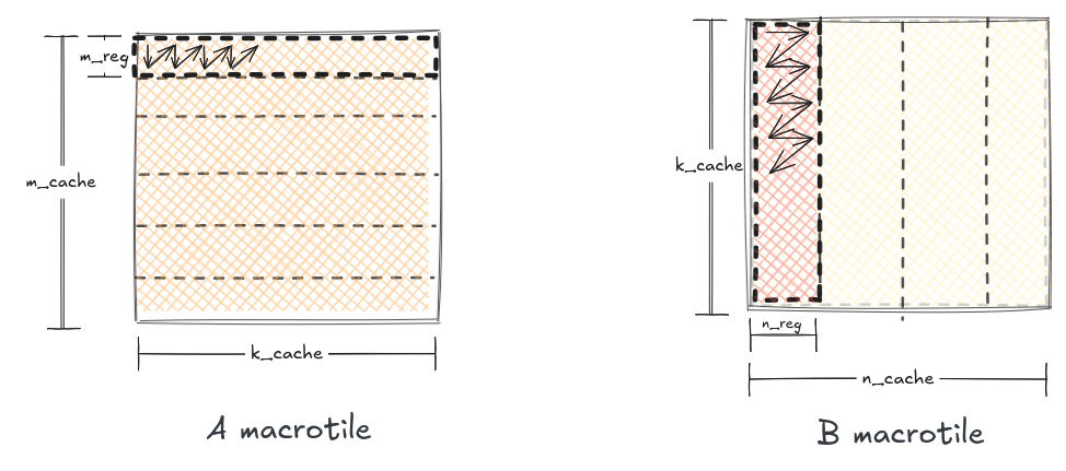
However, there’s one more consideration to make. Look at our access patterns within each macrotile. A’s panel is still not sequential, so we should pack each microtile column-major (transposed form). The B macrotile still suffers from a column stride, so we should pack block by block. Essentially, we pack in the order of accesses to play nice with the prefetcher and cache line sizes. 18
18 Don’t forget that even though the A and B macrotile are in L2 and L3, they still will be fetched into L1 anyways. This will definitely be a less significant improvement than caching from DRAM, but it is still worth noting.
It makes the code look like this:
#include "impls.hpp"
#include <cstdlib>

void packing_sequential(int M, int N, int K, const float *left,
                        const float *right, float *result) {
  constexpr int splitRowRegisters = 8;
  constexpr int splitColRegisters = 32;

  constexpr int splitRowCache = 512;
  constexpr int splitColCache = 1024;
  constexpr int splitInnerCache = 256;

  float *packA = (float *)aligned_alloc(64, splitRowCache * splitInnerCache *
                                                sizeof(float));
  float *packB = (float *)aligned_alloc(64, splitInnerCache * splitColCache *
                                                sizeof(float));

  for (int cc = 0; cc < N; cc += splitColCache) {
    for (int kc = 0; kc < K; kc += splitInnerCache) {

      // Pack everything into packB
      int idx = 0;
      for (int block = 0; block < splitColCache; block += splitColRegisters) {
        for (int j = 0; j < splitInnerCache; j++) {
          for (int i = 0; i < splitColRegisters; i++) {
            packB[idx] = right[(j + kc) * N + (i + cc + block)];
            idx++;
          }
        }
      }

      for (int rc = 0; rc < M; rc += splitRowCache) {

        // Pack everything into packA
        for (int block = 0; block < splitRowCache; block += splitRowRegisters) {
          for (int i = 0; i < splitRowRegisters; i++) {
            for (int j = 0; j < splitInnerCache; j++) {
              packA[block * splitInnerCache + j * splitRowRegisters + i] =
                  left[(i + rc + block) * K + (j + kc)];
            }
          }
        }

        // Macrokernel
        for (int c = cc; c < cc + splitColCache; c += splitColRegisters) {
          for (int r = rc; r < rc + splitRowCache; r += splitRowRegisters) {

            // Microkernel
            register_accumulator_sequential<splitRowRegisters,
                                            splitColRegisters / 16>(
                splitInnerCache, packA + (r - rc) * splitInnerCache,
                splitRowRegisters, packB + (c - cc) * splitInnerCache,
                splitColRegisters, result + r * N + c, N);
          }
        }
      }
    }
  }

  free(packA);
  free(packB);
}
and we also have some minor changes in the microkernel. But now its sequential access!
template <int m_reg, int n_reg>
inline void register_accumulator_sequential(int k_cache, const float *left,
                                            const int lda, const float *right,
                                            const int ldb, float *result,
                                            const int ldc) {
  __m512 acc[m_reg][n_reg];

  // Fill registers with the result
  for (int r = 0; r < m_reg; r++) {
    for (int c = 0; c < n_reg; c++) {
      acc[r][c] = _mm512_load_ps(result + r * ldc + c * 16);
    }
  }

  for (int i = 0; i < k_cache; i++) {

    // Load `columns` registers of `right`
    __m512 right_row[n_reg];
    for (int c = 0; c < n_reg; c++) {
      right_row[c] = _mm512_load_ps(right + i * ldb + c * 16);
    }

    // Actual matmul
    for (int r = 0; r < m_reg; r++) {
      __m512 el = _mm512_set1_ps(left[i * lda + r]);

      for (int c = 0; c < n_reg; c++) {
        acc[r][c] = _mm512_fmadd_ps(el, right_row[c], acc[r][c]);
      }
    }
  }

  // Move registers into memory
  for (int r = 0; r < m_reg; r++) {
    for (int c = 0; c < n_reg; c++) {
      _mm512_store_ps(result + r * ldc + c * 16, acc[r][c]);
    }
  }
}
Work Sharing
What multithreading gets you
My 9950X has 16 cores, and right now our implementations are only using 1 of them. Multithreading has it’s own traps: since we’re sharing memory across threads, we need a way to divide up the work to avoid race conditions.
The easiest way is to divide up work in a way so that they’ll only touch their section of C, so no locking + atomics are needed. We can choose to split work up through the rows or the columns: 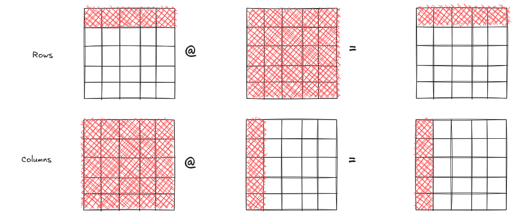
This choice is actually forced onto us 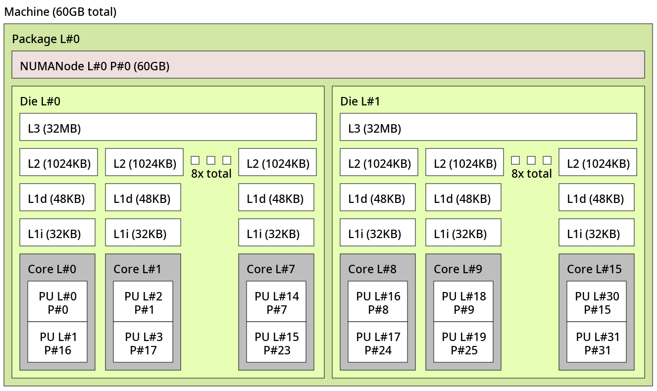
Since L3 is shared cache, our packB needs to be shared through all cores. So we’re forced to do the multithreading across rows, since our packB is determined by our column & k indexes.19 20
19 Some readers will point out that there are technically 2x32MB L3 caches. I tried to multithread by splitting the columns to each individual CCD, and then rows within each CCD but I couldn’t figure out how to get OpenMP to pin each thread to a specific core (or it genuinely might not actually be a speed up). I may revisit this in the future.
20 Nonetheless, being able to schedule across hardware units is very useful for a good BLAS library. Like my CCDs splitting cache up, bigger compute farms feature multiple sockets (separate CPUs). Multi-socket boards also use the Non-uniform memory access design, meaning that it’s actually very important to pin threads to a CPU, or you’d not only pay a cache miss but also a remote access penalty. This is because NUMA assigns RAM sticks to certain processors (their “local” memory), and any access to another processor’s assigned RAM stick (“remote” memory) will have to travel across a slower, higher latency bus. My PC is certainly no HPC setup, so I don’t have NUMA and can’t test it besides renting a cloud VM. Also may be worth visiting in the future.
We’ll use OpenMP to easily parallelize the regions.
#include "impls.hpp"
#include <cstdlib>

void parallel(const int M, const int N, const int K, const float *left,
              const float *right, float *result) {
  constexpr int splitRowRegisters = 8;
  constexpr int splitColRegisters = 32;

  constexpr int splitRowCache = 32;
  constexpr int splitColCache = 2048;
  constexpr int splitInnerCache = 1024;

  float *packB = (float *)aligned_alloc(64, splitInnerCache * splitColCache *
                                                sizeof(float));

#pragma omp parallel num_threads(16)
  {
    float *packA = (float *)aligned_alloc(64, splitRowCache * splitInnerCache *
                                                  sizeof(float));

    for (int cc = 0; cc < N; cc += splitColCache) {
      for (int kc = 0; kc < K; kc += splitInnerCache) {

#pragma omp for
        // Pack everything into packB
        for (int block = 0; block < splitColCache; block += splitColRegisters) {
          for (int j = 0; j < splitInnerCache; j++) {
            for (int i = 0; i < splitColRegisters; i++) {
              packB[block * splitInnerCache + j * splitColRegisters + i] =
                  right[(j + kc) * N + (i + cc + block)];
            }
          }
        }

#pragma omp for
        for (int rc = 0; rc < M; rc += splitRowCache) {

          // Pack everything into packA
          for (int block = 0; block < splitRowCache;
               block += splitRowRegisters) {
            for (int i = 0; i < splitRowRegisters; i++) {
              for (int j = 0; j < splitInnerCache; j++) {
                packA[block * splitInnerCache + j * splitRowRegisters + i] =
                    left[(i + rc + block) * K + (j + kc)];
              }
            }
          }

          // Macrokernel
          for (int c = cc; c < cc + splitColCache; c += splitColRegisters) {
            for (int r = rc; r < rc + splitRowCache; r += splitRowRegisters) {

              // Microkernel
              register_accumulator_sequential<splitRowRegisters,
                                              splitColRegisters / 16>(
                  splitInnerCache, packA + (r - rc) * splitInnerCache,
                  splitRowRegisters, packB + (c - cc) * splitInnerCache,
                  splitColRegisters, result + r * N + c, N);
            }
          }
        }
      }
    }
    free(packA);
  }
  free(packB);
}
We hoist the B block since all threads are meant to share it. We also wrap our entire kernel in a #pragma omp parallel num_threads(16). This allows us to have OpenMP spawn the threadpool once and reuse.
Some important things to point out:
#pragma omp for
// Pack everything into packB
for (int block = 0; block < splitColCache; block += splitColRegisters) {
  for (int j = 0; j < splitInnerCache; j++) {
    for (int i = 0; i < splitColRegisters; i++) {
      packB[block * splitInnerCache + j * splitColRegisters + i] =
          right[(j + kc) * N + (i + cc + block)];
    }
  }
}
We run packing in parallel as well! Yes, DRAM can run at 90 GB/s, but that number is not per-core. We can only reach top speeds if every single core is working on it, which is why we parallelize this operation too.
Also - I explicitly set it to num_threads(16)? But why not 32? Simultaenous multithreading splits each core into two threads, which allows for better utilization when the other thread is stalling for memory. But if we used it, it would fight with our cache lines (two different tiles would be assigned to one physical CPU core with only one set of L1/L2) and we only have 2 physical units for doing FMAs which are now contested between threads. So at best, not to slight improvement and at worst, cache eviction and even worse performance.
Due to multithreading - our parameters have to change. m_cache should be less than 4096 / 16 = 256 so that each of the 16 threads has work to do. And here, multithreading beats slightly better cache utilization.
Analytical vs Empircal Tuning
However, the parameters we were using this whole time are purely analytical. It’s important to benchmark the actual results. I made Google Benchmark sweep over the entire valid range of parameters for 4096x4096 matrixes.21
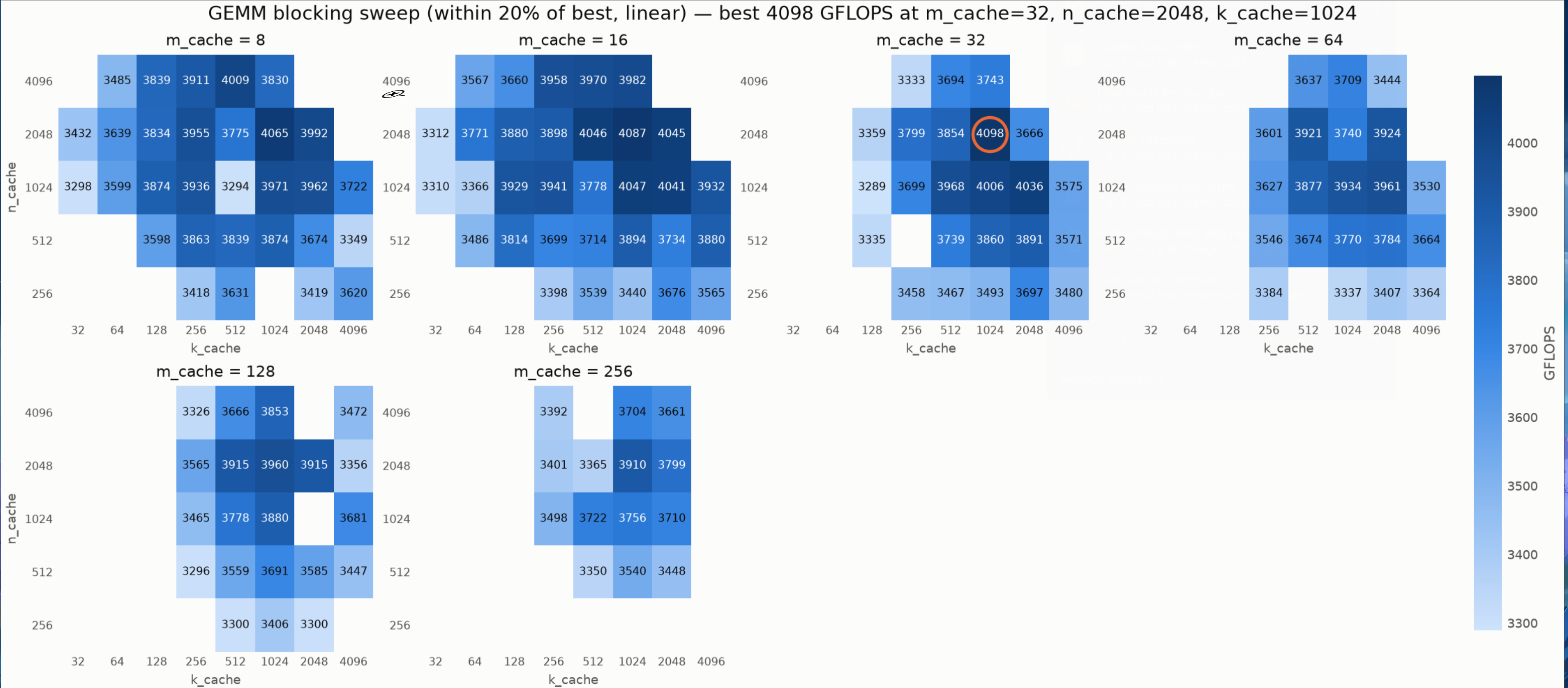
Seems like the best values are actually with a k_cache of greater than 256, which our analysis doesn’t predict! Previously, I mentioned that the C matrix will have to be touched K / k_cached times. So perhaps the model is optimizing for that. Another thing I didn’t consider was putting the B micropanel in L2. It is also technically streaming, as it’s reused value lives in registers. And L2 is fast enough to stream to our microkernel without any delays, so the model likely bumped it up to reduce the amount of K / k_cached extra touches to the C matrix.
m_cached being < 256 doesn’t necessarily surprise me. At that stage, we are no longer worrying about fitting in cache but how well we can parallelize. What was interesting, is that the model chose smaller values.
Checking on perf: 
| m_cache | parallel_autotune utilziation | packA (KB) | packB (KB) |
|---|---|---|---|
| 16 | 8.98% | 64 | 8192 |
| 32 | 9.47% | 128 | 8192 |
| 64 | 11.14% | 256 | 8192 |
| 128 | 12.53% | 512 | 8192 |
| 256 | 15.17% | 1024 | 8192 |
with k_cache=1024, n_cache=2048
It seems that we’re spending less time in the microkernel (doing actual math) and more time in the parallel_autotune. That either means a) our microkernel is getting slower or b) our packing is taking longer. And it likely has to do with our caches slowing down our microkernel. But as I mentioned now, our model no longer is exclusively holding L2 for packA, it’s also holding the microtiles. So it ends up being forced into L3. And we can see the jump from 128 -> 256 is huge (relative to the other, incremental jumps), because now the A panel is forced into some parts of L3.
Lastly, the biggest surprise was why it chose n_cache = 2048 and not 4096. My theory is that at lower levels, we’re actually re-using the C panel across the k / k_cache! 22 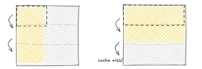
22 Yes, it’s not sequential memory but L3 has 32768 sets, so we don’t have any strided-access problem. So no need to pack C.
To see if this is true, we’ll measure 3 key statistics: instructions per cycle (IPC), L3 miss % and DRAM access. Instructions per cycle would show us any stalls in the execution pipeline (which will likely be the result of a cache miss). L3 Miss % and DRAM access will show us if there’s any trend in how L3 is used.
Measuring with perf stat -e cycles,instructions,ls_any_fills_from_sys.local_ccx,ls_any_fills_from_sys.dram_io_near23
23 Docs. L3 miss % is calculated by doing dram_io_near / (dram_io_near + local_ccx), which calculates how many L3 misses divided by total L3 hits + misses. This is using the property that the CPU only fetches from DRAM if it can’t find it in L3.
| n_cache | IPC | L3 miss % | DRAM / it |
|---|---|---|---|
| 1024 | 2.7 | 30.03% | 5067499 |
| 2048 | 2.7 | 28.43% | 4438079 |
| 4096 | 2.5 | 32.50% | 5859488 |
We can see a pattern: it hits a cliff at 4096 and drops. It starts missing much more L3 caches, and starts fetching from DRAM more, which points to the original theory.
This just goes to show the limits of analytical modeling and how it’s important to test your findings!
Conclusion
We got to 4120 GFLOPS, which is 103% of what OpenBLAS can do!
Matrix multiplication is a fun exercise for exploring concepts about cache, memory behaviors, and fancy SIMD instructions.
To truly turn these into a GEMM library, there are thousand more factors we have to consider. Our writeup dealt with a fixed size but for a true, performant library they have to look at:
- Handle weird dimensions that aren’t a multiple of the cache dimensions (we cheated a bit here)
- Actually implement the
C = alpha * A @ B + beta * Cfunctionality of GEMM (we skipped this for simplicity of code) - Is thread spawn + join worth it for the size?
- Is packing worth it for the size?
- What should the values of
m_regandn_regbe for this specific microarch? - What should the values for
m_cache,n_cache,k_cachebe for specific CPUs and this specific size
As you can see, a lot of these questions are also based on the dimensions of the operands, the microarchitecture, differences between cache sizes, NUMA configurations. Making a BLAS library isn’t easy.
Thanks for reading!
Resources
- https://siboehm.com/articles/22/Fast-MMM-on-CPU: The inspiration
- https://dl.acm.org/doi/epdf/10.1145/2925987: This paper serves as most of the backbone for the 5-loop structure
- https://excalidraw.com/: For the visuals!